
NEET Physics is the scoring paper in the medical entrance examination. Here, you will discover the NEET Physics MCQ Questions for all Concepts as per the latest syllabus. Practice more on a regular basis with these NEET Physics objective questions on air pollution and improve your subject knowledge & problem-solving skills along with time management. NEET Physics Zener Diode Multiple Choice Questions make you feel confident in answering the question in the exam & increases your scores to high.
MCQs on Zener Diode
1. In a Zener diode with a high breakdown voltage has
(a) Lightly doped P and N
(b) P or N is lightly doped
(c) Heavily doped P and N
(d) None of these
Answer
Answer: (a) Lightly doped P and N
2. In Zener diode, the Zener breakdown takes place
(a) Below 6 V
(b) At 6 V
(c) Above 6 V
(d) None of the above
Answer
Answer: (a) Below 6 V
3. Which of the following controls the current in a Zener diode?
(a) Zener diode resistance
(b) Potential barrier
(c) Reverse bias voltage
(d) External circuits
Answer
Answer: (d) External circuits
4. A Zener diode when biased correctly
(a) a. Never overheats
(b) b. Has a constant voltage across it
(c) c. Acts as a fixed resistance
(d) d. Has a constant current passing through it
Answer
Answer: (c) Has a constant voltage across it
5. In Zener diode, the breakdown is due to Zener, has a doping
(a) Lowest
(b) Moderate
(c) High
(d) Low
Answer
Answer: (c) High
6. In a Zener diode
(a) Negative resistance characteristic exists
(b) Forward voltage rating is high
(c) Sharp breakdown occurs at a low reverse voltage
(d) All of the above
Answer
Answer: (c) Sharp breakdown occurs at a low reverse voltage
7. A Zener diode, having breakdown voltage equal to 15 V, is used in a voltage regulator circuit shown in the figure. The current through the diode is
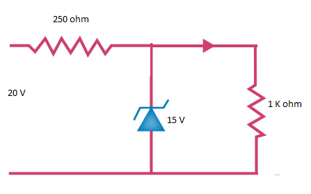
(a) 10 mA
(b) 15 mA
(c) 20 mA
(d) 5 mA
Answer
Answer: (d) 5 mA
8. How is the breakdown region set during the manufacturing of the diode?
(a) By controlling the size of the diode
(b) By controlling the doping of the diode
(c) By managing the biasing of diode
(d) All the above
Answer
Answer: (a) By controlling the doping of the diode
9. Depletion region behaves as
(a) Semiconductor
(b) Insulator
(c) Conductor
(d) High resistance
Answer
Answer: (B) Insulator
10. Depletion region contains
(a) Free holes
(b) Free electrons
(c) Immobile charge carriers
(d) All of the above
Answer
Answer: (c) Immobile charge carriers